The Atomic Force Microscope (AFM)
A rich variety of forces can be sensed by atomic force microscopy. In the non-contact mode (of distances greater than 10Å between the tip and the sample surface), Van der Waals, electrostatic, magnetic or capillary forces produce images of topography, whereas in the contact mode, ionic repulsion forces take the leading role. Because its operation does not require a current between the sample surface and the tip, the AFM can move into potential regions inaccessible to the Scanning Tunnelling Microscope (STM) or image fragile samples which would be damaged irreparably by the STM tunnelling current. Insulators, organic materials, biological macromolecules, polymers, ceramics and glasses are some of the many materials which can be imaged in different environments, such as liquids, vacuum, and low temperatures.
The basic objective of the operation of the AFM is to
measure the forces (at the atomic level) between a sharp probing tip
(which is attached to a cantilever spring) and a
sample surface. Images are taken by scanning the sample relative to the
probing tip and measuring the deflection of the cantilever as a function
of lateral position. Typical spring constants are between 0.001 to 100
N/m andmotions from microns to ~ 0.1Å are measured by the deflection
sensor. Typical forces between tip and sample range from 10e-11
to 10e-6N. For comparison the interaction between two covalently bonded
atoms is of the order of 10e-9N at separations of ~1Å.Therefore,
non-destructive imaging is possible with these small forces
[E. Meyer, Prog. Surf. Sci. 41, 3-49, (1992)]
The electromagnetic wavefield in solids and their surfaces plays an equal and complementary role to the electron wavefield, a role emphasised by recent experimental developments. Inverse photoemission observations from STM tips show detailed structure in the visible region of the spectrum having its origin in electromagnetic resonances between tip and the surface. In more conventional inverse photoemission (IPE) experiments, structure is dominated by surface electronic band structure. The same electromagnetic fields are responsible for forces acting at large distances between an AFM tip and the surface (in the non-contact mode). The electromagnetic field comes into its own in nanoscale structures. For atomic scale materials it remains firmly pinned to its origins in the electron charge but, given more space, develops a dynamics of its own, more properly described by Maxwell's equations than by the Schrodinger equation.
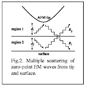
The force can be thought to
arise from changes in the zero-point energy of the electromagnetic
(EM) wavefield, which are caused by bringing the tip close to the
surface. When no observed surface is present, these waves are singly
scattered from the tip and escape to infinity. At the proximity of
the observed surface, however, the waves are multiply scattered between
the tip and the surface, thus modifying the net field, which implies a
change in the field energy i.e. a force (fig.2). To calculate it, we
need to know the reflection coefficient of the tip and of the surface
to incident electromagnetic waves. This is what our theory is set up to
do.
We have within our grasp a general formulation of electromagnetic effects in nanostructures based on reflection coefficients. One central theme will be the calculation of dispersion forces (a class of Van der Waals forces), but we can also treat problems of resonance enhanced IPE experiments. Having developed our methods we plan to solve the following problems:
- The force-distance law in the AFM, especially with application to lateral resolution as a function of distance. The theory can be formulated in exact parallel to our earlier STM theory with electron reflection coefficients replaced by photon reflection coefficients.
- Forces in systems where resonance enhancement is extreme: for example metal tips on rough silver surfaces as in the giant Raman resonance experiment.
- The influence of illumination by powerful laser beams on forces in the AFM, especially in highly resonant systems.
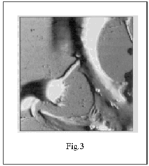
In fig.3, the AFM in biology: One
rapidly evolving area in scanning force microscopy is the construction
of tips to measure specific force interactions in cells. An exciting
future development would be the construction of antibody modified tips
that could measure or localise antigens on the surface of a cell
(by vertical/lateral force detection) or relocate them in the plasma
membrane. This would allow one to study the biophysics of molecular
interactions and its role in important processes such as
signal transduction, the process by which information flows throughout a
biological system. Here, an AFM image of living neurons and glia from
rat hippocampus [E. Henderson, Prog. Surf. Sci. 46, 1, 39-60 (1994)].